
Heat has become the physical limit AI hardware keeps running into, as conventional cooling struggles to keep pace with heat concentrated in denser and more complex packages. Atomica's new AI Thermal Microstructures Platform addresses that challenge as the fourth part of a broader AI infrastructure strategy focused on moving data, delivering optical power, integrating complex systems, and managing heat closer to where it is generated.
SANTA BARBARA, Calif., Aug. 25, 2026 /PRNewswire-ÌÇÐÄVlog/ -- , a U.S.-based microfabrication foundry, today announced the launch of its for customers developing thermal-management structures for high-density AI compute, advanced packaging, photonic systems, and other next-generation hardware. The platform follows Atomica's , , and Platforms.
Every generation of AI compute produces more heat in less space, intensifying thermal challenges inside dense packages. Traditional air cooling, heat sinks, cold plates, and data-center cooling remain essential, but localized heat and thermal gradients increasingly require solutions at the package level.
"That changes how thermal management has to be designed," said Eldon Klaassen, CEO of Atomica. "The industry has traditionally attacked the problem from the outside with heat sinks, cold plates, and airflow. As packages become denser, more of the thermal solution has to be built into the package itself."
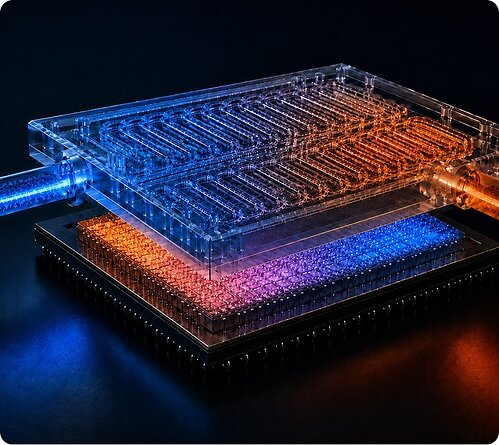
Atomica's AI Thermal Microstructures Platform combines microfluidic cooling, thermal pathways, interposers, sensing structures, bonding, and wafer-level packaging. These building blocks can route coolant near hotspots, spread heat, monitor pressure and flow, isolate temperature-sensitive components, and support integrated thermal control within advanced packages.
The platform supports applications including liquid-cooled AI accelerator modules, GPU and chiplet packages, high-bandwidth memory integration, photonic interposers, optical engines, co-packaged and near-packaged optics, external laser source systems, rugged edge-AI systems, industrial electronics, defense systems, and high-reliability sensor modules.
"The value is not in any one channel, via, interposer, or package feature," Klaassen said. "The harder challenge is combining those structures into a single architecture that can survive testing, qualification, and volume production. That is the integration and manufacturing challenge Atomica is built to solve."
Thermal management is also increasingly important in optical integration. As lasers and optical engines move closer to processors and switches, temperature gradients and thermal drift can affect performance and stability. Microfabricated thermal structures can help manage those effects within compact optical systems.
Customers can begin with feasibility structures or thermal test vehicles and progress through engineering samples, functional prototypes, qualification lots, and scalable production.
A new eBook describing the AI Thermal Microstructures Platform is available at .
About Atomica
is a U.S.-based microfabrication foundry that builds advanced platforms for AI hardware, photonics, sensors, MEMS, and biotechnology devices.
Atomica delivers rapid prototyping and scalable production to customers developing AI optical connectivity, AI optical source integration, AI photonic integration, AI thermal microstructures, physical AI sensors, MEMS optical control systems, and biotechnology microdevices.
Atomica operates a 30,000-square-foot Class 100 cleanroom near Santa Barbara, California, supporting a wide range of capabilities and materials with ISO 9001 certification and ITAR registration. Capabilities include photolithography, deposition, dry etch, wet etch, bonding, plating, metrology, testing, dicing, and planarization.
Atomica leverages engineering collaboration, process standardization, modeling and simulation, artificial intelligence optimization, and proprietary fab technology to achieve customer objectives.
Media Contact
Stephen Bohn, Atomica Corp., 1 805-696-6181, [email protected],
SOURCE Atomica Corp.

Share this article